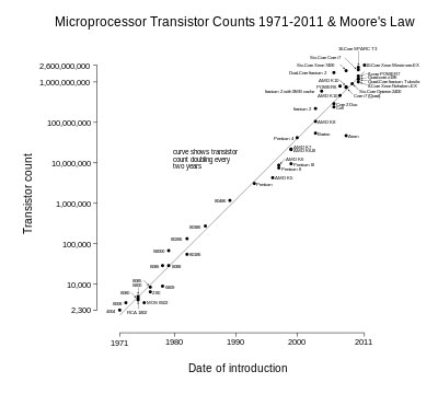
" Moore’s
law – the observation that the number of transistors in a dense
integrated circuit doubles approximately every 18 to 24 months – is a
projection and not a physical or natural law. Nonetheless, it has proved
accurate for several decades, and has been used in the semiconductor
industry to guide long-term planning and to set targets for research and
development.
Many
advances in digital electronics are strongly linked to Moore’s law:
examples are quality-adjusted microprocessor prices, memory capacity,
sensors and even the number and size of pixels in digital cameras.
But
can this continue indefinitely? Intel stated in 2015 that the pace of
advancement has slowed, starting at the 22nm feature width around 2012,
and continuing at 14nm. However, in April 2016, Intel CEO Brian Krzanich
stated that “In my 34 years in the semiconductor industry, I have
witnessed the advertised death of Moore’s Law no less than four times.
As we progress from 14nm technology to 10nm and plan for 7nm and 5nm and
even beyond, our plans are proof that Moore’s Law is alive and well”.
Physical limits
Silicon-based
technologies have nearly reached the physical limits of the number and
size of transistors that can be crammed into one chip, while alternative
technologies are still far from mass implementation. Down-scaling
transistor size is more than an engineering challenge, as there is
fundamental physics to consider.
Moore’s
law would come to an end because transistors are as small as atoms and
cannot be shrunk any further. To address this, fundamentally new
concepts for electronics would be needed to produce commercially viable
alternatives which meet demands for ever-growing computing power.
Moore’s Law may become exhausted eventually unless new technologies come
along that will lend it leash.
“The
whole semiconductor industry wants to keep Moore’s Law going. We need
better performing transistors as we continue down-scaling, and
transistors based on silicon won’t give us improvements anymore,” said
Heinz Schmid, a researcher with IBM Research GmbH at Zurich Research
Laboratory in Switzerland.
Compound semiconductor materials
Schmid’s
Zurich-based team with support from colleagues in Yorktown Heights, New
York has developed a relatively simple, robust and versatile process
for growing crystals made from compound semiconductor materials that
will allow them be integrated onto silicon wafers – an important step
toward making future computer chips that will allow integrated circuits
to continue shrinking in size and cost even as they increase in
performance.
The
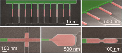
IBM team has fabricated single crystal nanostructures, such as
nanowires, nanostructures containing constrictions, and cross junctions,
as well as 3-D stacked nanowires, made with so-called III–V materials.
Made from alloys of indium, gallium and arsenide, III-V semiconductors
are seen as a possible future material for computer chips, but only if
they can be successfully integrated onto silicon. So far efforts at
integration have not been very successful.
The
new crystals were grown using an approach called template-assisted
selective epitaxy (TASE) using metal organic chemical vapour deposition,
which basically starts from a small area and evolves into a much
larger, defect-free crystal. This approach allowed them to
lithographically define oxide templates and fill them via epitaxy, in
the end making nanowires, cross junctions, nanostructures containing
constrictions and 3-D stacked nanowires using the already established
scaled processes of Si technology.
“What
sets this work apart from other methods is that the compound
semiconductor does not contain detrimental defects, and that the process
is fully compatible with current chip fabrication technology,” said
Schmid. “Importantly the method is also economically viable.”
Spin not charge
One
promising approach to developing new technologies is to exploit the
electron’s tiny magnetic moment, or ‘spin’. Electrons have two
properties – charge and spin – and although current technologies use
charge, it is thought that spin-based technologies have the potential to
outperform the “charge-based” technology of semiconductors for the
storage and process of information.
Scientists
from University College London (UCL) have discovered a new method to
efficiently generate and control currents based on the magnetic nature
of electrons in semi-conducting materials, offering a radical way to
develop a new generation of electronic devices.
In
order to utilise electron spins for electronics, or ‘spintronics’, the
method of electrically generating and detecting spins needs to be
efficient so the devices can process the spin information with low-power
consumption. One way to achieve this is by the spin-Hall effect, which
is being researched by scientists who are keen to understand the
mechanisms of the effect, but also which materials optimise its
efficiency. If research into this effect is successful, it will open the
door to new technologies.
The
spin-Hall effect helps generate ‘spin currents’ which enable spin
information transfer without the flow of electric charge currents.
Unlike other concepts that harness electrons, spin current can transfer
information without causing heat from the electric charge, which – as
mentioned above – is a serious problem for current semiconductor
devices. Effective use of spins generated by the spin-Hall effect can
also revolutionise spin-based memory applications.
The
scientists have reported a 40-times-larger effect than previously
achieved in semiconductor materials, with the largest value measured
comparable to a record high value of the spin-Hall effect observed in
heavy metals such as platinum. This demonstrates that future spintronics
might not need to rely on expensive, rare, heavy metals for efficiency,
but relatively cheap materials can be used to process spin information
with low-power consumption.
Touch and Go
Overall,
perpetuating Moore’s Law in the foreseeable future will require the
development of disruptive technologies which take the electronics
industry beyond its silicon comfort zone. Whether these can be developed
in time for Moore’s Law to be maintained in the immediate future is
touch and go, but even if not, there is no reason why it could not
resume in the future"


